


 |
4000V MOV Protection Device , 230pF Sensitive Components Chip Varistor
Product Details:
| Place of Origin: | DONGGUAN,GUANGDONG,CHINA |
| Brand Name: | JYVDR |
| Certification: | CQC,UL1449,TUV |
| Model Number: | JYVDR-10D511K |
Payment & Shipping Terms:
| Minimum Order Quantity: | 10000PCS |
|---|---|
| Price: | 0.06-0.08 USD/PC |
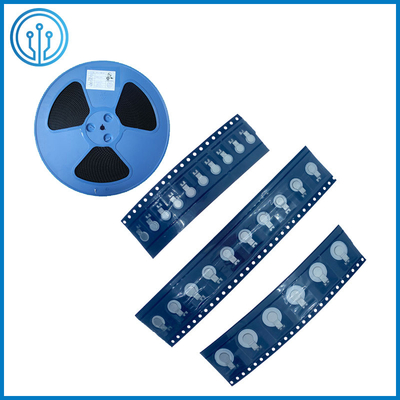
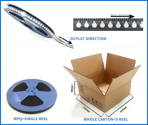
| Packaging Details: | Tape,1500pcs per reel,7500pcs per carton,12kg per carton,40*39*19cm |
| Delivery Time: | 7-10 Workdays |
| Payment Terms: | TT IN ADVANCE |
| Supply Ability: | 100,000,000PCS PER MONTH |
|
Detail Information |
|||
| Name: | Chip Varistor | Varistor Voltage: | 510V±10% |
|---|---|---|---|
| VAC: | 325V | VDC: | 415V |
| Max Energy: | 2.0KA (4000V) | Max Power: | 0.4W |
| Operating Temperature: | -40~125℃ | Max Capacitance: | 230pF |
| CQC: | CQC18001203056 | UL1449 4th Ed: | E481249 |
| TUV: | B 094255 0002 Rev.00 | SGS: | CANEC2121716206 |
| Storage Temperature: | -40~+85℃ | Relative Humidity: | ≤95% |
| High Light: | 4000V MOV Protection Device,230pF MOV Protection Device,Chip Metal Oxide Varistor |
||
Product Description
Sensitive Components Chip Varistor 10D511K 510V For Surge Overvoltage Protection
Introduction Of The Chip Varistor 10D511K
MLA (Multilayer Varistor), SMD transient voltage suppressor, also known as zinc oxide varistor or "surge absorbers", is a kind of voltage and current-voltage properties of symmetric properties resistors. MLA is semiconducting ceramics (zinc oxide) for materials through lamination technology (multi-layer) manufacturing, with excellent instantaneous energy absorption capacity, as well as fast internal thermal fugitive character, to achieve the effect of protection circuit, also known as multilayer varistor.
![]()
Features Of The Chip Varistor 10D511K
* Encapsulated packages, SMD type.
* Colorful enclosure, matching with LED lighting fixtures overall product design.
* RoHS REACH compliant
* Available for SMT flow/reflow soldering
* Low profile and space saving
* Large capability to withstand high surge current
* Low inductance construction with excellent response
* Encapsulation material according to UL94-V0
* Operating temperature range: -40°C ~ +85°C
* Storage temperature range: -40°C ~ +125°C
* Agency recognition: UL/cUL.CQC,TUV
Recommended Applications Of The Chip Varistor 10D511K
* Suitable for LED lighting driver application.
* Switching power supply.
* Power strips,wall adapters
* Power supply
* Home appliance
* Industrial equipment
* Telecommunication or telephone system
Customer Services Of The Chip Varistor 10D511K
* Customized design and production.
* ODM / OEM
* Surge protective countermeasures for terminal equipment.
* Trial run for surge standard requirements.
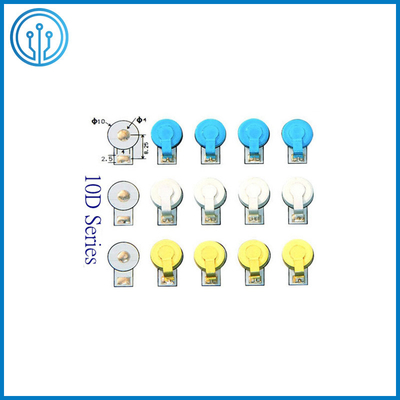
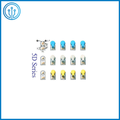
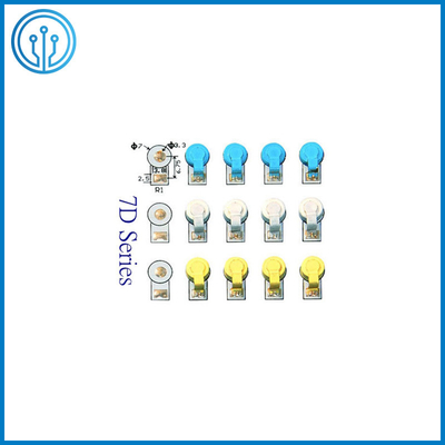
Dimension Of The Chip Varistor 10D511K
![]()
![]()
| Model JYVDR~ |
Pad A | Pad B | Pad center distance C | Diameter D | Height H±1.0 | Thickness T | |
| Φa | b1 | b2 | |||||
| 10D271 | 4.0 | 4.0 | 2.5 | 8.25 | 10.0 | 14.2 | 2.0 |
| 10D471 10D511 10D561 | 3.0 | ||||||
| 05D 07D 10D All series use 15-inch reel and 24-inch feeder placement machine | |||||||
Highly Recommended:
1. In the drawing board, it is recommended that the A solder joint be used as the L line, the B solder joint
as the N line, and the copper skin connected to the B solder joint is routed around the pressure-sensitive
chip circle (the entire diameter D should be regarded as belonging to the A solder joint.
2. For the sake of safety arcing, the circular edge of the chip should be at least 2.5mm away from any
other conductive device, as shown in the figure above (in order to prevent mutual displacement with
other devices during patching, if the space allows, please reserve the larger the interval is. Okay.)
3. The use of varistors in DC circuits has unfavorable factors. It is not recommended to use varistors in
rectified DC circuits. Please consider carefully or contact our company at 18128566098
(sales1@ampfort.net), thank you!
Specification Of The Chip Varistor 10D511K
| Model JYVDR~ |
Varistor Voltage | Max Allowable Voltage | Max Clamp Voltage(8/20us) | Max Energy | Max Static Power | Capacitance | ||
| VDC | VAC | VDC | VDC | IP | Combined wave(A) | W | pF | |
| 10D271 | 270±10% | 170 | 220 | 450 | 35A | 2.0KA(4000V) | 0.4 | 380 |
| 10D471 | 470±10% | 300 | 380 | 760 | 40A | 250 | ||
| 10D511 | 510±10% | 325 | 415 | 835 | 230 | |||
| 10D561 | 560±10% | 350 | 450 | 920 | 210 | |||
For different voltage application environments, we recommend the following pressure sensitive
combinations to provide overvoltage, surge and lightning stroke protection for ACLED.
| Working Voltage Environment |
Forestage Varistor Parameter | Back-end Varistor Parameter | Remarks |
| 110VAC±20% | 270VDC±10% | / | In view of the insufficient voltage withstand capability of the IC, the two-stage varistor can be upgraded to 4KV lightning protection. The user can choose the varistor size according to the requirements of the anti-surge level. |
| 220-230VAC±20% | 510VDC±10% | 470VDC±10% | |
| 240VAC±20% | 560VDC±10% | 510VDC±10% | The combination is recommended for users in Indian and Brazil. |
Because the varistor is easy to deteriorate in an environment with large voltage fluctuations, the varistor
voltage should be selected as much as possible under the premise that the IC (MOS tube) + lamp bead
on the lamp board has a sufficient withstand voltage and the voltage fluctuation area is large. A
combination with a higher value should be selected, and a varistor with a large flow and a large size
should be selected as far as possible under the premise of the cost.
Certifications Of The Chip Varistor 10D511K
| Certification | CHINA | CQC | GB/T10193-1997 | 05D:CQC18001202949 07D:CQC18001202948 10D:CQC18001203056 |
| USA/Canada | UL | UL1449 | E481249-20180122 | |
| Germany (EU) | TUV | IEC61051 | B 094255 0002 Rev.00 | |
| ROHS | SGS/SVHC | SGS is updated annually SVHC is effective for a long time |
05DSGS:CANEC2121716202 07DSGS:CANEC2121716204 10DSGS:CANEC2121716206 SVHC:CANEC2200885702 |
Package Of The Chip Varistor 10D511K
| Model JYVDR~ |
MPQ (QTY/REEL) (PIECES) | WEIGHT/REEL(KG) | QTY PER REEL(PIECES) | WEIGHT PER CARTON(KG) |
| 05D271 | 4000 | 1.5 | 20000 | 8 |
| 05D471 | 3000 | 1.5 | 15000 | 8.4 |
| 05D511 | 3000 | 1.5 | 15000 | 8.4 |
| 07D271 | 3000 | 1.8 | 15000 | 9.5 |
| 07D471 | 2000 | 1.7 | 10000 | 9.1 |
| 07D511 | 2000 | 1.7 | 10000 | 9.1 |
| 07D561 | 2000 | 1.7 | 10000 | 9.1 |
| 10D271 | 2000 | 2 | 10000 | 11 |
| 10D471 | 1500 | 2.2 | 7500 | 12 |
| 10D511 | 1500 | 2.2 | 7500 | 12 |
| 10D561 | 1500 | 2.2 | 7500 | 12 |
Appendix II: Form of Pulse Derating Curve
| Specificati on/Model | Pulse Width | 50us | 100us | 500us | |||||||||
| Current | 5A | 10A | 50A | 100A | 5A | 10A | 50A | 100A | 5A | 10A | 50A | 100A | |
| 05D | Times | 104 | 102 | X | X | 102 | 10 | X | X | 10 | X | X | X |
| 07D | 106 | 104 | 2 | X | 105 | 103 | X | X | 102 | 2 | X | X | |
| 10D | ∞ | ∞ | 103 | 10 | ∞ | 105 | 102 | 2 | 106 | 103 | 1 | X | |
| 14D | ∞ | ∞ | 104 | 103 | ∞ | 106 | 103 | 102 | 106 | 104 | 2 | 1 | |
| 20D | ∞ | ∞ | 105 | 104 | ∞ | ∞ | 104 | 103 | ∞ | 106 | 103 | 101 | |
![]()